MAC5 TECHNICAL SERVICES PROJECTS
Mac5 Technical Services has built a research team with over 75 years of experience with the Department of Energy through their prime contractors at Oak Ridge National Laboratory and the Y-12 National Nuclear Security Complex. Mac5’s laboratory facility is located in Oak Ridge, TN and has capabilities to conduct high temperature materials experiments and analyze material composition. Mac5 performs and guides research and development activities in various areas of materials and manufacturing technology development and manufacturing development solutions.
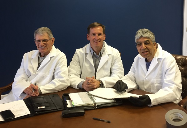
Our team consists of world class PhD’s, formerly program leaders with the Y-12 National Security Complex and Oak Ridge National Laboratory (ORNL) – Dr. Roland Seals and Dr. Vinod Sikka. Dr. Seals is an experienced materials and coatings chemist with over 39 years of experience. Dr. Sikka is a former division manager with over forty years of experience. Below are brief summaries of Dr. Seals and Dr. Sikka’s experience:

Dr. Roland Seals
Formerly Chief R&D Technical Consultant & Senior Scientist at the Y-12 National Security Complex
PhD in Chemistry with over 39 years of experience at Y-12
Holds 23 issued patents and has 7 patents pending
Highlighted Inventions and Patents
FTIR spectrometer with solid-state drive system (1999)
Condensed phase conversion and growth of nanorods instead of from vapor (2005)
Anchored nanostructure materials and method of fabrication (2012)
Nanostructured composite reinforced material (2012)
Method of fabrication of anchored nanostructure materials (2013)
Method of producing catalytic materials for fabricating nanostructures (2013)
Heat treatment furnace (2014)
Toughened and corrosion- and wear-resistant composite structures and fabrication (2014)
Composite materials formed with anchored nanostructures (2015)
Nano-material and method of fabrication (2015)
Dr. Vinod Sikka
Formerly Manager of Research & Technology Development at ORNL
PhD in Metallurgical Engineering with over 40 years of experience
Over 200 publications in journals and conference proceedings
60 patents issued and 4 pending
16 R&D 100 Award Winner
Specialties include:
alloy design, high-temperature properties, and commercial applications
developing new research technology development and funding opportunities
developing advanced materials for structural applications
developing novel methods for processing of materials
developing new processing equipment
transfer of technology developed from the research to industry
Dr. Neal Evans
Scanning Electron Microscopy Specialists
PhD materials scientist with over 30 years of experience in characterization of nanostructured alloys, ceramics, electronic and biological materials
Over 60 publications
2014 AIME Champion H. Mathewson Medal Award
2011 R&D 100 Award
Excellence in Technology Transfer - 2007
2006 R&D 100 Award
2006 Federal Laboratory Consortium (FLC) Southeast Region Award for Excellence in
Scanning Electron Microscopy Capabilities
Currently, Mac5 has arrangements to access the state-of-the-art fully analytical scanning electrons microscopes that are within the Joint Institute for Advanced Materials, University of Tennessee Knoxville. Conventional metallurgical mounts, either prepared by Mac5 or provided to Mac5 in a ready-to-examine condition, as well as larger components which require sectioning, can be accommodated.
Zeiss EVO MA15 Scanning Electron Microscope
1. Electron beam operation from 0.1 to 30 keV
2. W or LaB6 emitters
3. Secondary electron (SE) and backscattered electron (BSE) imaging modes
4. Variable pressure mode of operation permits examination of non-conducting samples
5. Bruker xFlash 6130 permits Energy Dispersive X-Ray Spectroscopy (EDS) using stationary probes, along user-defined lines and full elemental maps
6. Bruker eFlash Electron Backscattered Detector permits Orientation Imaging Microscopy (OIM)
A Zeiss Auriga Dual Beam FIB/SEM provides additional complementary capabilities:
Focussed Ion Beam Operation
1. Gallium liquid metal ion source
2. Resolution is 7 nm at 30kV acceleration voltage
3. Acceleration voltage 5-30 kV
4. Single Source Gas Injection system
Scanning Electron Microscope Capabilities
1. FEG electron source
2. Resolution 1 nm at 15 kV and 1.9 nm at 1kV
3. Acceleration Voltage 0.1 to 15 kV
4. Secondary electron (SE) and backscattered electron (BSE) imaging modes
5. STEM capabilities for low-voltage transmission imaging
a. Four-quadrant dark field annular detector
b. Bright field detector
